en
en
 English
 繁体中文
繁体中文 Japanese
 Korean
 Russian
 German
News
Deepen Optoelectronic Resources, Lead Technological Breakthroughs

Deepen Optoelectronic Resources, Lead Technological Breakthroughs
1、 Overview of Terahertz (THz) Technology
Terahertz waves refer to electromagnetic waves with frequencies ranging from 0.1 to 10 THz (wavelength 30 μ m-3 mm), between microwave and infrared, and were once known as the "THz Gap" due to technological limitations. Its core features include:
(1) Low photon energy: Only at the millielectronvolt level, with no risk of ionizing radiation, suitable for biological live detection.
(2) Strong penetrability: It can penetrate non-polar materials such as plastics, ceramics, and fabrics, but strongly reflects metals and is strongly absorbed by water molecules.
(3) Molecular fingerprint spectrum: The vibrational/rotational energy levels of organic macromolecules (such as DNA and explosives) are in the THz band, which can identify the composition of the substance.
(4) High resolution: The spatial resolution reaches sub millimeter level (such as resolving tank surface scratches at 3.5 cm), and the temporal resolution reaches picosecond level.
2、 Characteristics and Technical Principles of High Resistance Zone Fused Silicon (HRFZ Si) Super Hemisphere Lens
Material characteristics
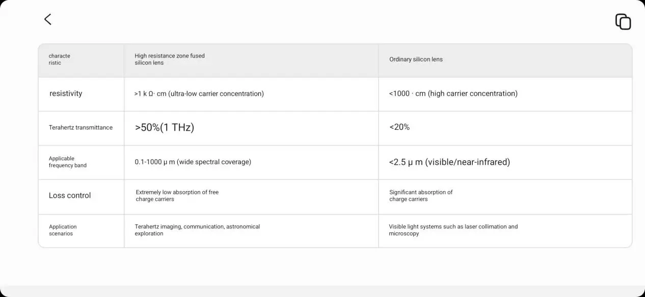
-High resistivity (>1 k Ω· cm): purified by zone melting method, impurity concentration<10 ¹² cm ⁻ ³, significantly reducing free carrier absorption in the terahertz band, with a transmittance>50% (1 THz), while ordinary silicon has a transmittance<20% due to carrier absorption.
-Wide band transmittance: covering 0.1-1000 μ m (near-infrared to millimeter wave), especially at 0.35-2.5 μ m with a transmittance>85%.
-High refractive index (n ≈ 3.45): Optimize terahertz wave focusing efficiency and enhance optical coupling capability.
Optical structure design
-Super hemispherical curvature: The curvature radius is greater than that of a hemisphere, providing a larger light collection angle and shorter focal length, reducing spherical aberration.
-Wavefront control: the traditional lens needs to be equipped with a parabolic mirror for secondary focusing, while the super hemisphere structure can directly converge divergent spherical waves into small angle conical waves (34 ° divergence angle), simplifying the optical path.
Technical bottlenecks and improvements
-Reflection loss: The silicon air interface has high reflectivity and requires coating with a terahertz high transmittance film (such as poly (p-xylene)) to increase the transmittance to ≥ 90%.
-Integrated Replacement: The new dielectric metasurface lens (composed of high resistance silicon micro pillar arrays) has a thickness of only 150 μ m and is directly integrated onto the antenna surface, replacing traditional bulky lenses.
3、 Application Fields
(1) Terahertz wave coupling and transmission
-Antenna integration: As a coupling element of photoconductive antenna (PCA), it collimates divergent spherical waves into quasi planar waves, improving signal transmission efficiency.
-Fiber optic communication: used for THz fiber endface lenses to reduce interface reflection losses and support 6G satellite communication (theoretical speed of 10 GB/s).
(2) High resolution imaging
-Security check and quality inspection: Penetrating plastic and paper to detect explosives and drugs inside packages (combined with THz fingerprint library).
-Biomedical: Early detection of dental caries (with an 80% improvement in accuracy compared to X-rays), identification of skin cancer tissue.
-Military detection: Identify disguised targets in dust/smoke environments, and detect human activities through wall penetrating radar.
(3) Astronomy and scientific research
-Detecting THz radiation such as carbon and water molecules in the universe to fill the gap in ground-based observations.
4、 Difference from ordinary silicon super hemispherical lens
Core Differences:
High resistance silicon is purified by zone melting to reduce impurities, while ordinary silicon (such as CZ growth) contains oxygen and carbon impurities that exacerbate losses; Its high resistivity directly suppresses terahertz wave absorption, while ordinary silicon experiences a sharp drop in transmittance due to its high carrier concentration.
Summarize
Terahertz technology has enormous potential in imaging, communication, and military fields due to its secure penetration and molecular fingerprint recognition capabilities; As the core optical component, the high resistance fused silicon hyper hemispherical lens solves the efficient coupling problem of terahertz waves through low loss materials and hyper hemispherical structures. Future trends include:
-Integration: Metasurface lenses replace traditional bulk optics to achieve chip level THz systems;
-Intelligence: Combining AI to optimize imaging algorithms (such as 3D reconstruction of Sanxingdui cultural relics);
-Multifunctional: Tunable lens extends the application of THz in scenarios such as in vivo biological detection and 6G dynamic beam control.
Calcium fluoride (CaF2) crystals play an irreplaceable role in the high-end optical field due to their unique optical properties. Its core advantages lie in its deep ultraviolet transmission capability and optical isotropy (without birefringence), making it the preferred material in multiple key fields.
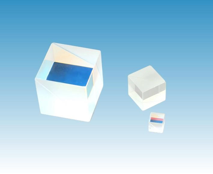
The cubic spectroscopic prism is an optical component with special geometric shape and optical properties, which is usually used for spectral analysis, refraction or changing the direction of light propagation.
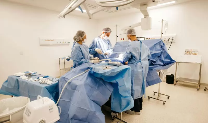
3D endoscope technology has become one of the indispensable and important tools in modern medicine. It enables doctors to observe and manipulate organs and tissues in the patient's body in real-time during surgery by utilizing advanced optical and imaging technologies.